

Technology Project
Hertz

Objective:
Benefit from the advantages of additive-generative manufacturing for generating antenna structures directly on the contact pads of microchips
Partners:

Duration: 01.11.2017 - 31.10.2019
Goals for the project

The goals of the Hertz project are twofold:
1. development of micro monopole antennas (diameter: 25 -100 µm, length: 375 µm) for frequency ranges from 100 GHz to 300 GHz by means of additive manufacturing processes such as laser powder cladding (LPA) and aerosol printing
2. process development for printing dielectric lenses directly on printed circuit boards with already integrated semiconductor chip for signal amplification
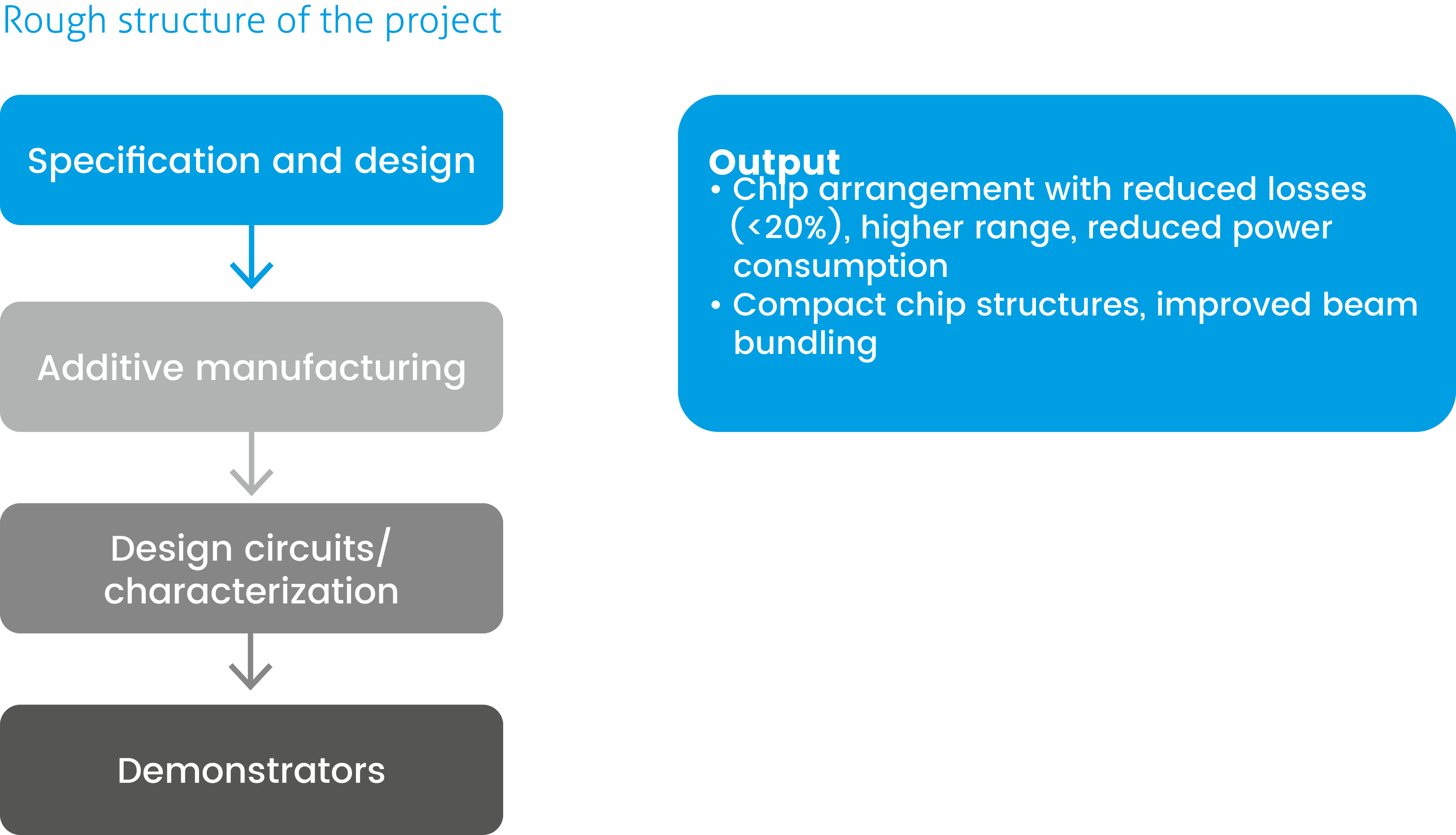
Interim project results
Micro monopole antennas
Professorship for Circuit Engineering and Network Theory, TU Dresden
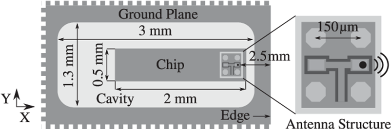
The aim is to develop an integrated receiver at 200 GHz for ultra-broadband communication up to 40 Gbit/s. By generating a 3D antenna directly on the chips, losses can be reduced and consequently the range and efficiency increased.
This project also includes the design and characterisation of the relevant circuit components, including a frequency multiplier, low-noise amplifier and down-mixer. The circuit development is already well advanced and allows to start first work for the implementation of the demonstrator. At the end of the project a functional setup with the self-developed components and integrated antennas should be available. At the same time, the state of the art is to be advanced so that the results obtained can also serve as a basis for future projects. This also supports the position of the TU Dresden and the Chair of Circuit Engineering as one of the leading institutions in this research area.
Fraunhofer IWS
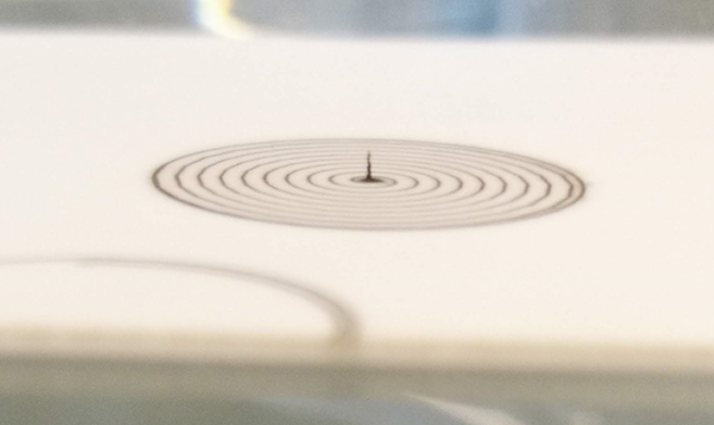
The first monopoly structures made of colloidal silver ink could be printed using aerosol printing. The height of the structures can be adjusted in a defined way up to a height of approx. 500 µm. The aerosol printing process allows the antenna structures to be produced at low process temperatures (approx. 90 °C).
Current development focuses on reducing the "overspray" on the antenna base and improving the mechanical stability of the structures.
Based on this, the antennas are mounted directly on the microchips (area approx. 1 mm² with a contact pad area for the antennas of approx. 80 x 80 µm). Subsequently, the electronic characterization is carried out at the TU Dresden using demonstrator chips. In addition, rod antennas were manufactured using laser powder cladding (LPA). The challenge still to be solved here includes the precise control of the heat input into the substrate (chip), which occurs during the melting of the powder particles supplied.
Dielectric lenses
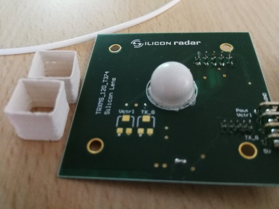
Silicon Radar
Special high performance silicon-germanium chips are developed, which are in direct contact with dielectric lenses by printing the lenses adapted to the chip geometry. This results in extremely compact dimensions, such as those used on small drones with radar sensors. For testing radar systems with printed lenses, test circuit boards are developed on which the radar chips are brought together with the lenses and their function and performance is verified. After this fundamental research, a wide range of applications are possible.
So far, two radar chips have been developed that operate at very high frequencies of 120GHz and 300GHz respectively. Due to the high frequencies the antennas can be integrated into the chip and due to the large bandwidth very accurate measurements can be performed. It has been shown experimentally that despite the small dimensions of a few millimeters, ranges of more than 10 meters can be achieved and that accuracies for layer thickness measurements in the micrometer range are possible. Initially, silicon lenses were used for the measurements. In the further course of the project these will be replaced by printed lenses, some of which are already available.
Fraunhofer IWS
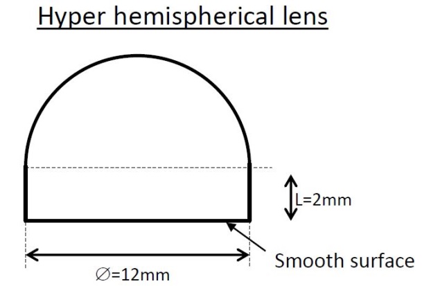
The required hyperspherical lenses are manufactured using the FFF (Fused Filament Fabrication) process. This requires a material with a high dielectric constant (ε ~ 10). The process development includes printing hyperspherical lenses with ABS (low ε), PVDF (medium to high ε) and with a special filament (very high ε). Further attention is paid to the process-side optimization of the surface waviness in situ as well as post situ after FFF printing (with as little "warping" effect as possible). Due to the clearly different flow behaviour of the special filament compared to ABS or PLA, the parameter optimisation is much more demanding. In the next project phase, optimized lenses will be delivered to Silicon Radar and tested for their suitability for use.
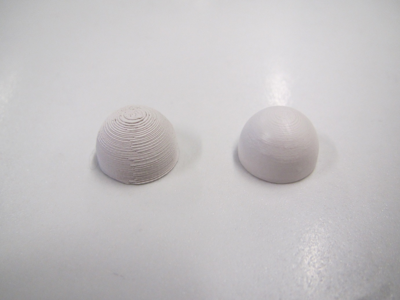
Lens structures printed with a high-ε filament after printing (left) and after smoothing (right). Diameter of the base area 12 mm.
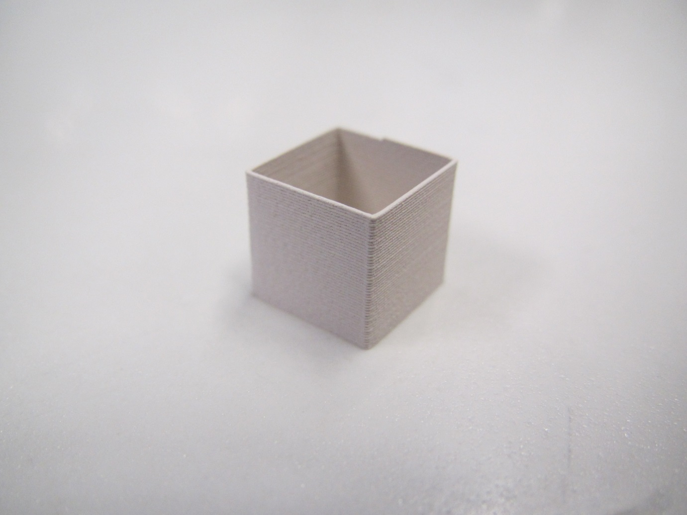
Structure for parameter optimization printed from special filament with ε ~ 10 (edge length 10 mm)